One focus of NaMLab’s research is the transfer of promising research results into real world applications. NaMLab is currently working together with its industrial partner GlobalFoundries towards to integration of the RFET concept into its 22 nm fully-depleted silicon-on-insulator (FDSOI) platform to serve as potential add-on technology. Here, the structural similarities of RFETs with FDSOI transistors are beneficial for the ease of co-integration. In principle, the same materials and processes can be used and no additional mask sets with critical dimensions are needed.

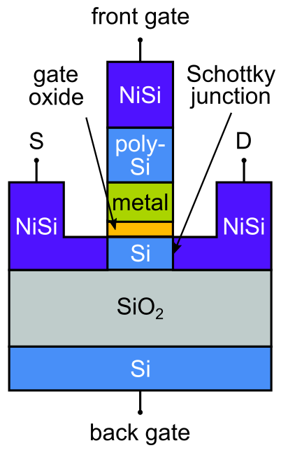
In this framework, a new back-bias (BB) RFET device concept was conceived. Instead of multiple independent front gates, the inherently present back-gate is used for programming here, leading to demonstration of the worlds smallest RFET with only 20 nm gate lengths and 80 nm width. Most process integration modules are shared with the n-FETs of the baseline technology, such as STI, hybrid etch, gate-first high-k metal gate (HKMG) front gate integration, and the complete BEOL. Modified S/D terminals are used to create silicide-to-semiconductor junctions in close proximity to the doping-free channel region (Fig.1).
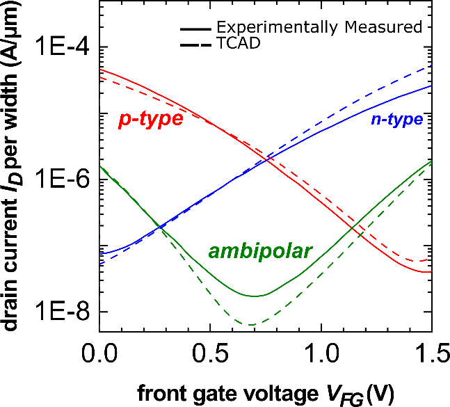
In the BB-RFET concept, we exploit the body-bias effect in FDSOI to adjust the carrier transport controlled by the front gate (FG) electrode. Different to other concepts, both front and back gate capacitively couple to the whole channel region. The applied VBB defines which charge carriers are injected into the active region for a given bias point of the front gate. This way, the whole transfer characteristic is shifted reversibly between the three different operation modes: p-type, ambipolar, and n-type. TCAD and Verilog models mimicking the device behavior were created as shown in Fig. 2.

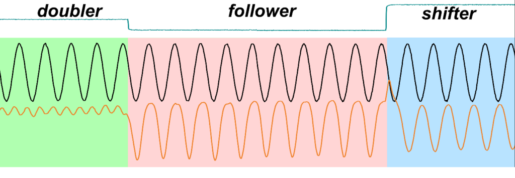
The new device concept is interesting for analog signal processing in wireless communication or integrated sensing systems. For example, a single transistor can be used for frequency doubling by exploiting the symmetric parabolic shape of the ambipolar mode, as illustrated in Fig. 3. By varying the applied back-bias the same circuit can be reconfigured to either signal follower or phase shifter, depending on the selected mode of the RFET. From this concept, a single-transistor binary-phase-shift-keying circuit (BPSK) can be derived. Using our simulation models also other single transistor analog building blocks, such as a reconfigurable half-wave and full-wave rectifier have been proposed.

Cooperation:
Globalfoundries Fab 1 Dresden (Germany), TU Darmstadt (Germany)

