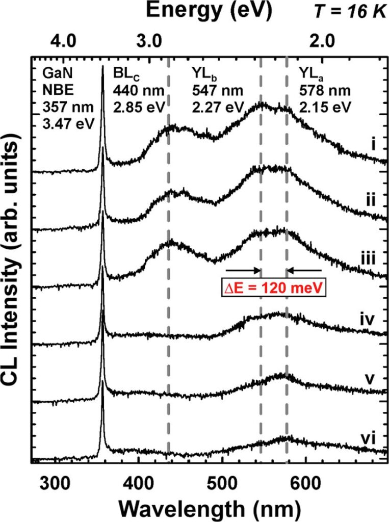
During the past years the growth of ultra-pure GaN/AlGaN heterostructures with atomically-smooth interfaces and surfaces on bulk GaN by molecular beam epitaxy (MBE) was established. The resulting layer stacks are a perfect reference system for fundamental material investigations as well as a test ground for novel electrical and optical device concepts. In particular, the role of carbon incorporation in GaN was re-visited. Carbon is a deep acceptor in GaN and historically considered to result in an impurity band around 2.2eV in photoluminescence studies, known as yellow luminescence (YL). Several years ago, it was already realized, that YL is also detected from GaN with no or a low level of incorporated carbon. Cathodoluminescence investigations at low temperature inside a transmission electron microscope (TEM) revealed, that two YL bands can be detected from carbon-doped GaN, while one around 2.15eV is also present for intrinsic material (Fig. 1). YL results from carbon incorporation, but in intrinsic material there must be a hitherto unknown deep acceptor present, which also results in a YL band. This unknown deep acceptor has a similar binding energy as carbon, reflected in the difference of 120meV between the two YL bands.

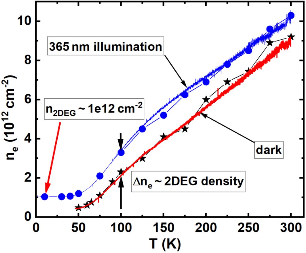
GaN/AlGaN stacks hosting a two-dimensional electron gas (2DEG) are the prerequisite for lateral field-effect transistor (FET) operation. Parasitic conduction paths in these stacks deteriorate FET performance, since the 2DEG cannot fully be depleted and thus the transistor cannot be turned off. Parasitic conductivity results from silicon at the substrate/MBE interface and originates from the adhesion of particles when the substrate is exposed to ambient atmosphere prior to loading for the subsequent overgrowth. Silicon acts as a shallow donor in GaN and the resulting free charges could in principle be compensated by a deep acceptor. In the present case, a carbon layer at the substrate/MBE interface was introduced to compensate the parasitic conductivity. It was shown that at low temperature the 2DEG is the only conducting channel and any parasitic conduction path was suppressed (Fig. 2). In this specific layer stack, the 2DEG is only present under illumination with ultra-violet (UV) light. Thus, magneto-transport measurements performed in the dark and under UV exposure allow for the separation of the density contribution from the 2DEG and the parasitic channel. Further it was demonstrated, that the density difference in the dark and under UV exposure is constant over the entire temperature range and thus the 2DEG density does not depend on the temperature.

Cooperation:
Max-Planck-Institute for Chemical Physics of Solids Dresden (Germany), TU Dresden (IHM) (Germany), Otto-von-Guericke Universität Magdeburg (Germany)

