OVERVIEW DIELECTRICS
Materials with high dielectric constant (high-k materials) play an increasingly important role in nanoelectronic devices. For example, in conventional semiconductors charge is stored in capacitors with a dielectric insulation layer. In order to maintain the storage capacity of capacitors, new dielectric materials with higher dielectric constants have to be introduced for devices with smaller area. Similar dielectric materials are needed for the next generation of high performance transistor devices as well as processors and logic products. A variety of research projects in the nano-scale regime are ongoing in order to gain an understanding of the influence of material properties with respect to leakage mechanisms, performance, speed and reliability.
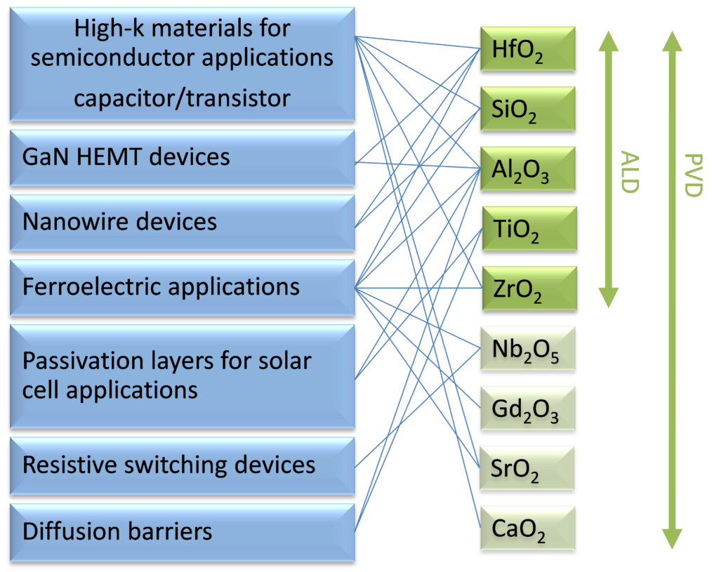
As depicted in the schematic below, a set of five main material systems (Al2O3, HfO2, ZrO2, TiO2, and SiO2) is used for different dielectric applications. Accordingly, a detailed understanding of the structural and electrical properties gained on a device application can be used as a fundamental basic knowledge for future new devices. The impact of process properties on the device performance can be correlated. Especially, the optimization of charges and traps, dielectric constants, material properties like density, dielectric, piezoelectric, ferroelectric, and optical properties are important for the various device applications.

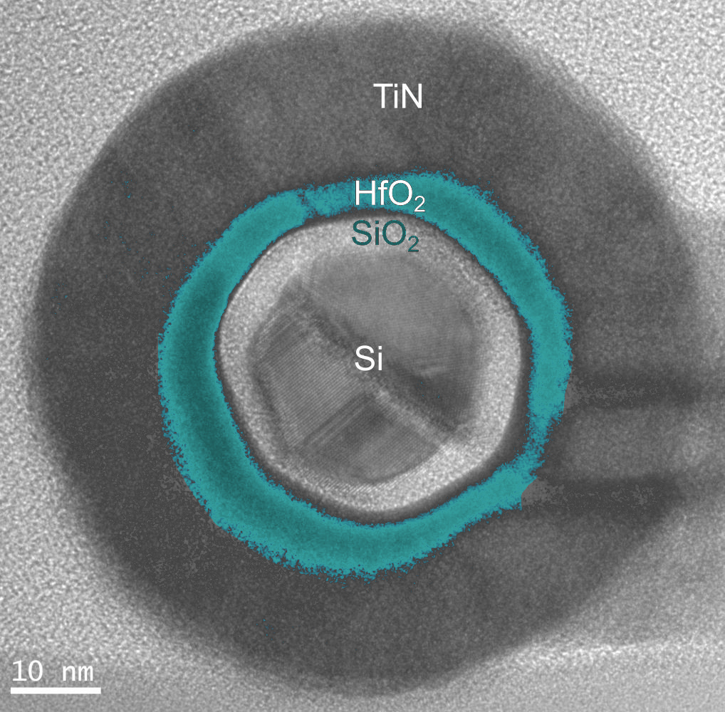
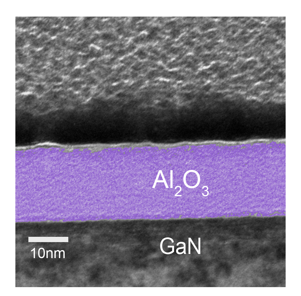
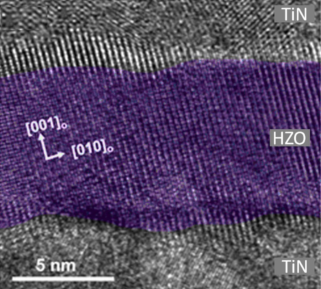
NaMLab also screens and characterizes other candidate materials for novel device applications, such as Nb2O5, La2O3, SrO2, Sc2O3, and CaTiO3. Additional novel dielectrics will follow. Materials are deposited by Atomic Layer Deposition (ALD), Physical Vapor Deposition (PVD), Chemical Vapor Deposition (CVD), and Molecular Beam Deposition (MBD), as shown in the drawing above. Research at NaMLab covers a wide range of applications, from dielectrics for nanowire transistors (Fig. 1), GaN HEMT devices (Fig. 2), to ferroelectric Hf0.5Zr0.5O2 based capacitors (Fig. 3).


