Most of NaMLab technologies are available for services. E.g., the research programs at NaMLab require very specific preparation of samples. The sample preparation ranges from low-complexity approaches of 1D layer stack depositions up to complex BEOL-post processing of functional devices on top of CMOS substrates using up to 5 lithography steps.
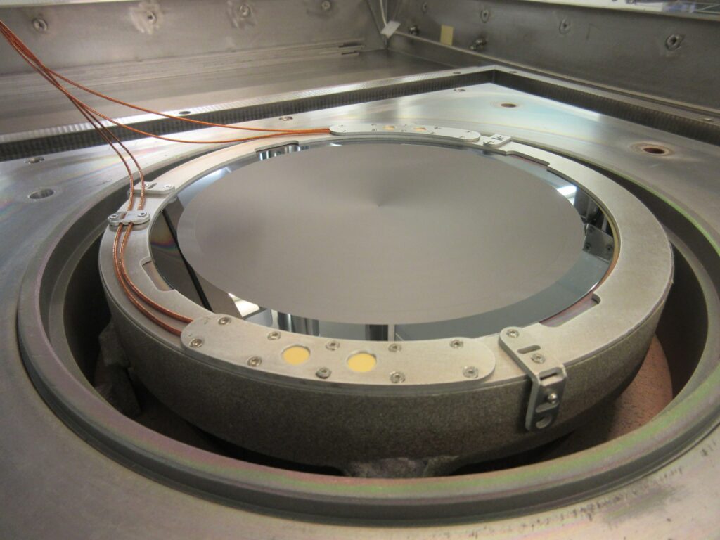
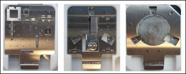
This preparation can include deposition of thin films and layers, thermal treatment of samples, patterning by lithography and etching, as well as sample cutting, grinding, polishing and engravings. For this purpose, the 330 m² ISO class 6 cleanroom facility includes various types of deposition tools: physical vapor deposition (PVD), atomic layer deposition (ALD) (Fig. 1), chemical vapor deposition (CVD), and molecular beam epitaxy (MBE). Post-deposition anneals can be performed up to 1200°C for fast anneals. There are fast ramping Rapid Thermal Processing machines available as well as furnaces for long-term treatment. Structures in the range of micro- and nanometers can be manufactured by employing shadow masking and lithographic methods like electron beam (Fig. 2) and laser lithography. The removal of the material includes wet chemical and reactive ion etching (RIE).
Additional processing requirements are adapting wafer geometries, chip dicing and creation of process compatible gadgets e.g. for sample handling. Therefore, NaMLab provides several tools to meet these requirements. A 300 W Laser cutter is located in NaMLab’s clean room. It offers the possibility to process wafers with diameters up to 300 mm and substrate thicknesses up to 1 mm. Via a CNC based vacuum chuck any 2-dimensional shape can be produced. This technique is used for dicing silicon wafers or cutting out small pieces without destroying processed and reusable wafers.
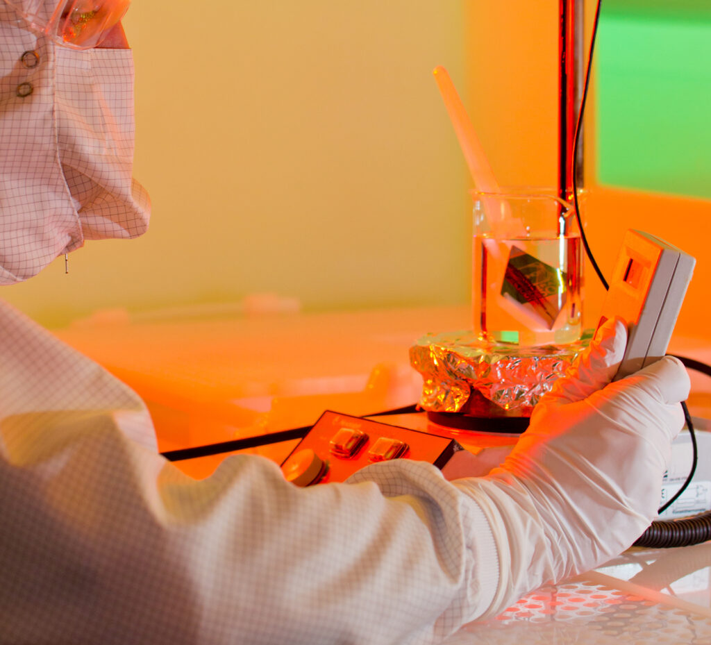
For cleaning and wet chemical treatment of samples, NaMLab owns four wet benches equipped with overflow basins (Fig. 3). They are located in an ISO class 5 cleanroom. Ultrasonic and megasonic tools for mechanical supported surface cleaning in deionized water are in operation. Also cleaning steps like RCA clean and selective material etching can be performed.
Tool overview (excerpt):
Sample and Wafer Processing by Atomic Layer Deposition for metals and oxides, Chemical Vapor Deposition, Sputter Deposition, Molecular Beam Epitaxy, Reactive Ion Etching (RIE, ICP), Rapid Thermal Annealing, Laser Lithography and Electron Beam Lithography
Analysis by Atomic Force Microscope, Ellipsometer, X-ray, SEM with EBSD and EDX
Electrical Characterisation by semi-automated and full-automated (300 mm) prober systems