The development of novel microelectronic devices as well as the scaling of existing devices concepts is tightly linked to the availability of mature and reliable integration of new dielectrics. On the nanometer scale those materials act as gate insulator, stress or strain layers or memory dielectrics. NaMLab performs electrical stress measurements on a large variety of devices to assess the reliability of the used dielectric materials. Moreover, simulation and modeling of the different degradation effects give deeper insight into the physical mechanisms. For an example, we have conducted a study reversible capture and emission processes of interface and oxide traps in a carbon nanotube (CNT) FETs by using pulsed measurement schemes. The measured data was then fitted by one of our partners using transient simulations with a CNT-FET compact model containing a trap modeling adjunct network with different time constants for capture and emission of processes exemplarily shown in Fig. 1.

In face of the increasing complexity of power devices or high performance logic devices any compromise in reliability is not acceptable. Especially for high dielectric constant gate insulators, the fundamental understanding of bias temperature instability (BTI), hot carrier injection (HCI), stress induced leakage currents (SILC), and time dependent dielectric breakdown (TDDB) are of major interest. To further deepen the understanding of use-case realistic stress conditions we put additional focus on the assessment of circuit reliability. That is, besides the standard reliability tests on single devices that are typically performed with high statistics at our partners premises, more advanced and time consuming characterization methods are investigated at NaMLab.

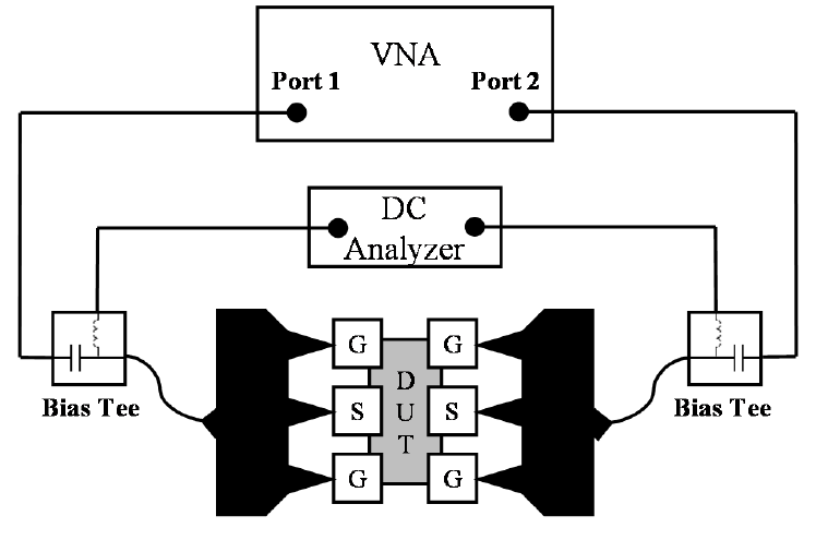
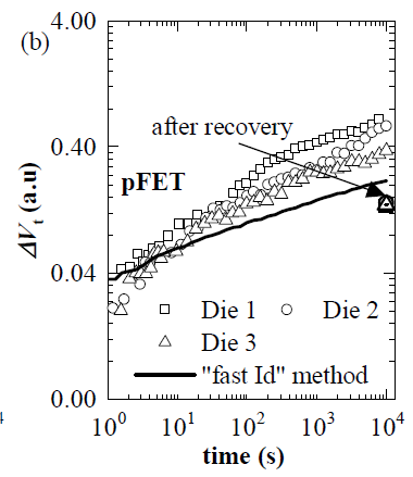
The growing interest in high speed and RF technologies assert for the importance of reliability characterization beyond the conventional DC or AC methodology. Power amplifiers for example that are adopted to realize on-chip transmitters have to operate stable at frequencies well beyond the GHz range. Thus, the correct understanding of degradation mechanisms that affect the RF device parameters becomes increasingly important. Often new methods have to be established to yield the desired information. For example, we have proposed a new S-Parameter based BTI characterization method, whose setup is shown in Fig. 2. This technique distinguishes itself from other BTI characterization methods, that it does not constitute any recovery component as the degradation is monitored without disengaging the stress condition while using a standard RF measurement setup. Exemplarily, the threshold voltage shift of a p-FET under BTI stress conditions is shown in Fig. 3. Data from S-Parameter based method is compared to the classical ‘fast ID’ method, as well as to the data achieved after a recovery time of a few minutes.


